
 Add as a preferred source on Google
Applied Materials Opens $5 Billion EPIC Semiconductor Research Center
The Sunnyvale facility will bring chipmakers, equipment companies, university researchers and Applied Materials engineers together to advance semiconductor research in the AI era.

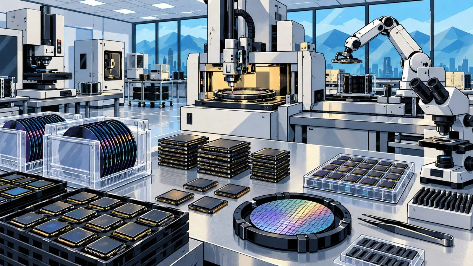
Applied Materials opened its Equipment and Process Innovation and Commercialization Center in Sunnyvale, California, on Oct. 12, bringing chipmakers, equipment companies, university researchers and its engineers together to advance semiconductor research in the AI era.
The company describes the center as a $5 billion capital investment, with spending expected to grow as customer projects begin. Its goal is to move semiconductor technologies toward high-volume manufacturing faster, though no development-time reduction was specified.
The 600,000-square-foot facility includes nearly four acres of advanced cleanroom space. Construction required more than six million hours.
Founding chipmaker partners include TSMC, Intel, SK hynix, Micron and Samsung Electronics. Other innovation partners include Broadcom, Advantest, SCREEN, KIOXIA and Besi, along with five university research partners.
The center is intended for collaborative research and development on semiconductor processes and manufacturing equipment. It is not a commercial chip production facility.
The opening builds on Applied Materials’ earlier announcement of the EPIC Center. Applied Materials reported $9.115 billion in revenue for its fiscal third quarter ended July 26, up 25% from a year earlier.
John Kim
John Kim reports on the digital-asset business for TokenPost. Send corrections or tips to info@tokenpost.com.