
 Add as a preferred source on Google
SK Hynix Plans $654 Million Semiconductor Test Center in South Korea
Trinity Fab is expected to open in May 2027 with about 50 tools for testing 12-inch wafers under production-like conditions.
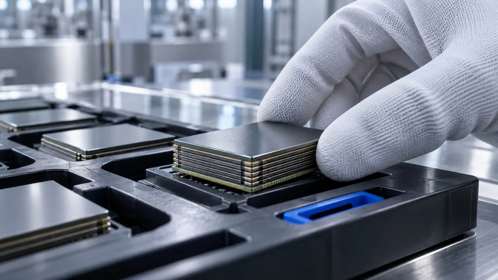
SK hynix plans to invest 874.6 billion won, or about $654 million, and work with the South Korean government to build a semiconductor test center in Yongin.
The center, named Trinity Fab, is expected to open in May 2027 with about 50 tools. Its equipment will include tools for lithography, etching and deposition, and the facility will provide a testing environment for 12-inch wafers.
The center is intended for South Korean small and midsize suppliers of chip materials and equipment. They will be able to assess product performance and yield in conditions similar to commercial production. Production-grade testing facilities are expensive and difficult to access, contributing to high validation costs and lengthy timelines for smaller suppliers.
An independent nonprofit foundation is expected to operate Trinity Fab to protect intellectual property. SK hynix describes it as the world’s first open test facility designed specifically to verify readiness for mass production.
John Kim
John Kim reports on the digital-asset business for TokenPost. Send corrections or tips to info@tokenpost.com.