
 Add as a preferred source on Google
UMC and Murata Pursue Separate Paths for Faster AI Optical Links
UMC and Wavetek are preparing foundry capacity on 6-inch and 8-inch wafers, while Murata’s modulator is designed for 400 Gbps per channel.

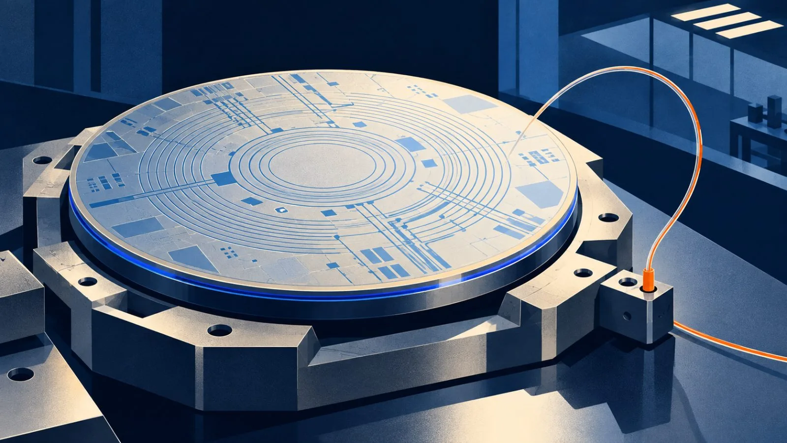
Two commercialization efforts are advancing thin-film lithium niobate (TFLN) for AI data-center optics: United Microelectronics Corporation (UMC) and Wavetek Microelectronics Corporation (Wavetek) are expanding foundry capacity as Murata Manufacturing Co., Ltd. develops a modulator.
UMC, Wavetek and HyperLight announced a partnership March 12, 2026, to produce HyperLight’s TFLN chiplet platform on 6-inch and 8-inch wafers. HyperLight designs the platform, while UMC and Wavetek provide foundry capacity. Wavetek has moved the technology onto a customer-qualified 6-inch CMOS line, and UMC is adding 8-inch capacity.
The platform is intended for data-center pluggable modules, long-distance coherent modules and co-packaged optics (CPO).
Murata’s June 2026 roadmap calls for initial TFLN modulator samples in the fourth quarter of 2026, followed by mass production in 2028. The device is designed for electro-optic bandwidth above 100 GHz and 400 Gbps per channel using PAM4. Murata also plans to develop proprietary technology for LNOI wafers and device processes, drawing on its lithium niobate materials and manufacturing experience with surface acoustic wave filters for mobile phones. Its broader CPO roadmap targets integration of optical, electrical and thermal functions by 2032.
A Marvell executive said at the AI Infra Summit that the rise from 224 Gbps to 448 Gbps per lane can make signal integrity a limit on copper’s reach. Optical connections are seeing greater use between server racks. The shift from 1.6 Tbps toward 3.2 Tbps also raises demands on modulator speed and power use.
TFLN is made by thinning single-crystal lithium niobate to hundreds of nanometers and bonding it to a base such as silicon or quartz. The resulting structure, lithium niobate on insulator (LNOI), is used to make modulators that encode electrical signals onto laser light. Voltage changes the material’s refractive index, which controls the light’s intensity or phase; the material does not carry light through the network.
High bandwidth, low optical loss and drive voltage that can approach CMOS levels make TFLN a candidate for 1.6 Tbps and 3.2 Tbps optical modules, coherent transmission and CPO. Manufacturing remains difficult: lithium niobate is hard to etch, and producing the thin film requires precise ion slicing. Long production timelines, unstable yields and advances in silicon photonics leave the technology’s scale-up uncertain. Murata’s first sample target is the fourth quarter of 2026.
Simon Yoon
ReporterSimon Yoon reports on blockchain technology for TokenPost. Send corrections or tips to info@tokenpost.com.