
 Add as a preferred source on Google
Intel Projects AI Chip Packages Could Reach 240 Millimeters Square
Intel foundry and packaging division official 李圭午 outlined larger package designs with at least 32 high-bandwidth memory stacks. Intel has not disclosed a production timetable or yield data for the largest projection.

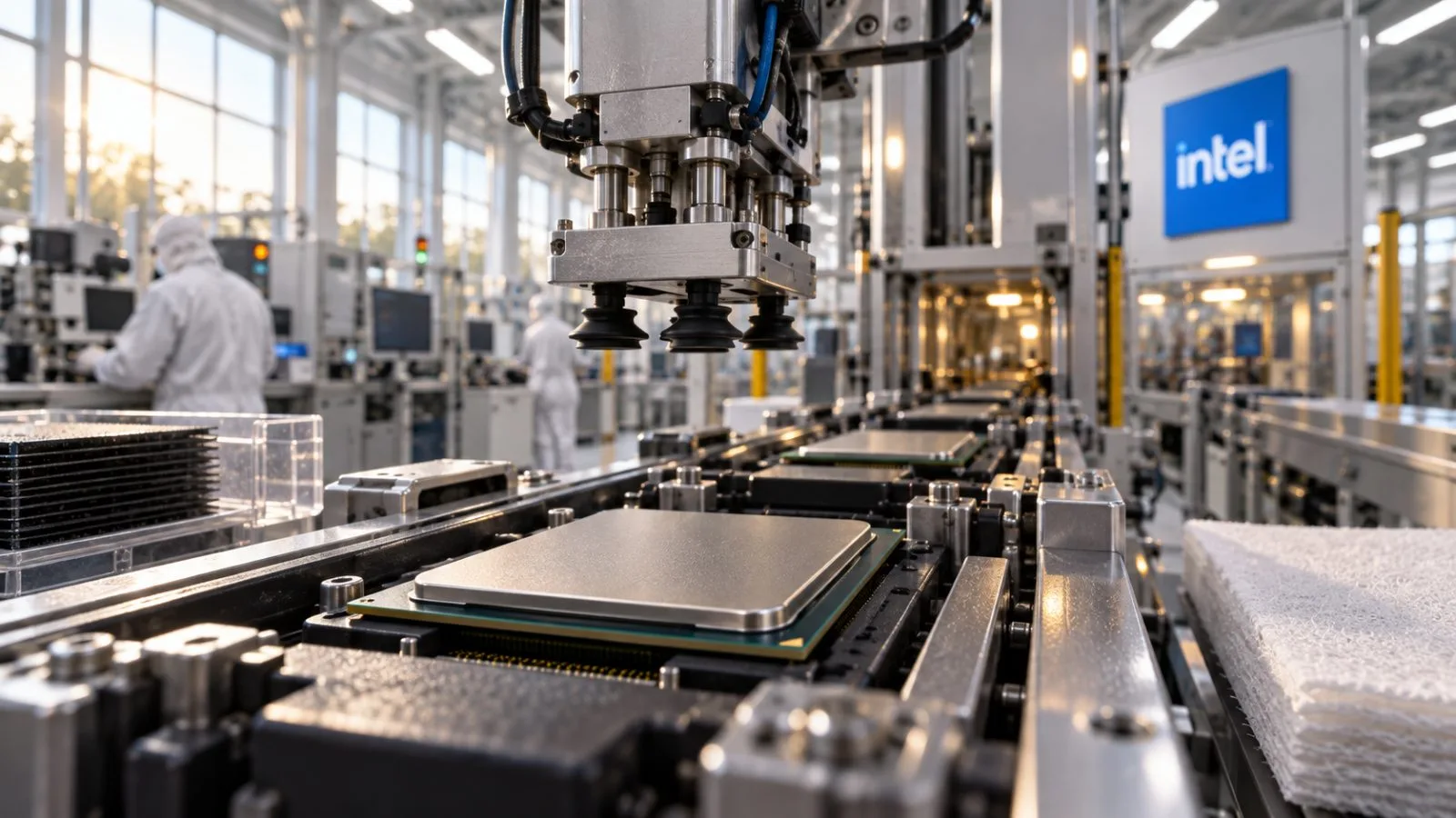
Intel projects that future AI chip packages could measure 240 by 240 millimeters, as manufacturers combine more computing chips and high-bandwidth memory (HBM) in a single package. The projection came from Intel foundry and packaging division official 李圭午 at ISMP 2026 in Busan on Nov. 4.
李圭午 described three package sizes. AI chips in commercial use this year can measure up to 120 by 120 millimeters, with 12 HBM stacks and at least 20 bridges. Designs under development measure at least 120 by 180 millimeters and use at least 16 HBM stacks and at least 38 bridges.
The projected 240-by-240-millimeter package would have at least 32 HBM stacks and at least 70 bridges. Its area would be four times that of the 120-by-120-millimeter design. More computing chips and memory in one package require connections between more components, increasing the number of bridges.
Intel’s Embedded Multi-die Interconnect Bridge (EMIB) places small silicon bridges where chips need dense connections, instead of using a full silicon interposer. The EMIB-T version adds through-silicon vias to the bridges to provide power-delivery paths.
Intel says its bridge design can use more than 90% of a silicon wafer, compared with about 60% for an interposer. The company has not disclosed a production timetable or yield and warpage data for packages at the projected size.
The projection does not establish that EMIB-T outperforms Taiwan Semiconductor Manufacturing Co.’s CoWoS packaging. TSMC’s CoWoS-L also uses localized silicon interconnects. CoWoS capacity remains tight as TSMC expands its advanced-packaging facilities.
Simon Yoon
ReporterSimon Yoon reports on blockchain technology for TokenPost. Send corrections or tips to info@tokenpost.com.