
 Add as a preferred source on Google
Diamond Foundry Shows 200-Millimeter Single-Crystal Diamond
The unpolished D200mm crystal was displayed at a conference in China and is not yet a finished wafer ready for chip fabrication.

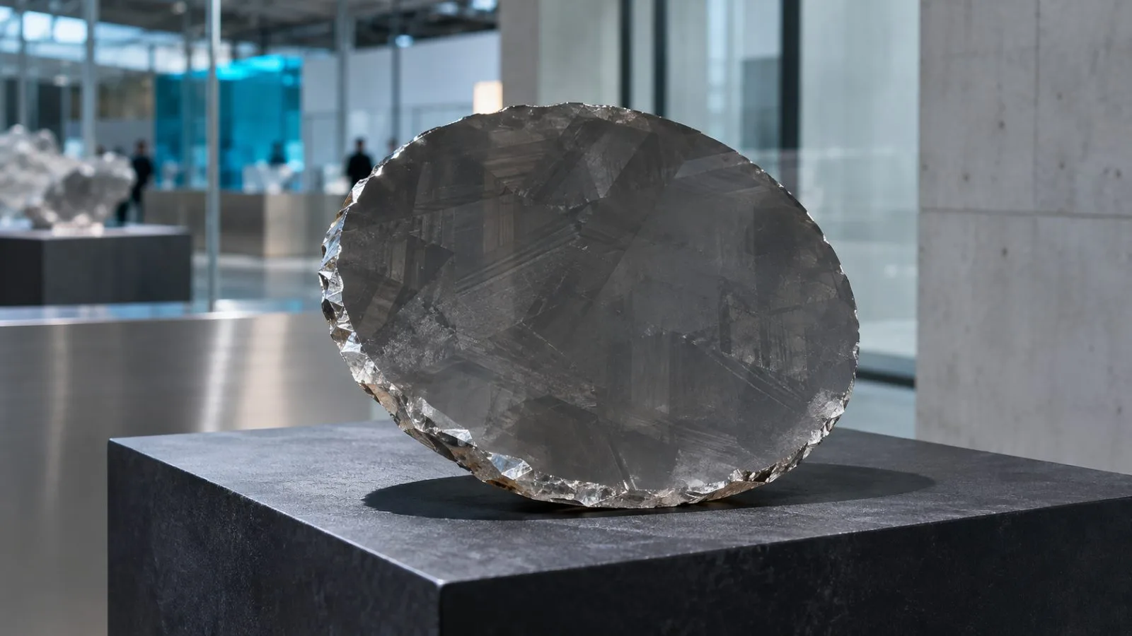
Diamond Foundry displayed a 200-millimeter single-crystal diamond at CarbonSemi 2026 in Ningbo, China, on Nov. 5-6, presenting a larger-format material aimed at heat management and power electronics.
The San Francisco company calls the crystal D200mm. Its diameter is twice that of the 100-millimeter single-crystal wafer Diamond Foundry announced in November 2023. The sample on display had not been polished and was not a completed wafer ready for fabrication.
D200mm has one continuous crystal structure, unlike polycrystalline diamond, which consists of many smaller crystals joined together. That structure makes the material a potential base for chips. Diamond’s thermal conductivity is about 2,000 watts per meter-kelvin, roughly five times copper’s.
Diamond Foundry is targeting cooling for high-power processors and smaller power electronics. The 200-millimeter format matches wafer dimensions used in chip production and could, in principle, fit existing manufacturing workflows. The company has not disclosed yield or defect-density data or how the material performs in commercial semiconductor processes.
Diamond Foundry is also developing a $2.77 billion production facility in Spain tied to the EU Chips Act. The displayed crystal marks a scale milestone, while its manufacturing performance remains unreported.
Simon Yoon
ReporterSimon Yoon reports on blockchain technology for TokenPost. Send corrections or tips to info@tokenpost.com.